 MENU
MENU 

EECS 413 students earn prizes for their final projects
“We were all impressed by the fact that most students chose highly-relevant and innovating projects,” stated Dr. Naraghi.
Students in EECS 413, Monolithic Amplifier Circuits, taught by Prof. Michael Flynn, presented their final projects in the Fall 2010 class, and two teams were awarded cash prizes for their designs by Cirrus Logic Inc.
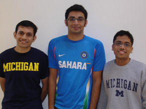
First place went to EE master’s students Karan Jain, Aswin Rao, and Abishek Madhavan for their project, “A High PSRR, Low Drop-Out Voltage Regulator using Feed-forward Ripple Cancellation,” Second place went to EE PhD studentsYejoong Kim, Dongsuk Jeon, and Suyoung Bang for the project, “A 1.2ps resolution, 76dB Dynamic Range Time-to-Digital Converter Based on a Tunable Vernier Delay Line.”
The class selected three finalists, and final selection was made by three judges from Cirrus Logic: Johann Gaboriau, Mixed-signal audio manager; Shahrzad Naraghi, (Ph.D. EE, U-M), Mixed-signal IC designer; and Virginia Ruff, University relations.
Dr. Naraghi stated, “We were all impressed by the fact that most students chose highly-relevant and innovating projects. A few of them had really challenging specifications somewhat comparable to cutting-edge ICs in the industry. For us, it was quite difficult to select the top projects. We simply liked all of them!”
First Place
A High PSRR, Low Drop-Out Voltage Regulator using Feed-forward Ripple Cancellation
 Enlarge
Aswin Rao, Abishek Madhavan, Karan Singh Jain
Background: There is a lot of interest in efficient power-management integrated circuits. Effective voltage regulation has become critical in low-power applications and in applications with widely varying environmental conditions. Especially in the low power design space, such as laptops and cellular phones, tight supply voltage requirements and multiple voltage domains make voltage regulation quintessential to the lifetime and performance of the system.
Project: This team presented a high power-supply rejection (PSR), high bandwidth low drop-out (LDO) voltage regulator using feed-forward ripple cancellation. The architecture provides a PVT-tolerant design with high PSRR of 50dB for a wide range of frequencies. This LDO has been implemented in 0.13μm CMOS technology and has a die area of 0.0078 mm2.
Results obtained show a line regulation of 0.45 mV/V and a load regulation of 0.06 mV/mA. The overall quiescent current consumption for the LDO is 55μA and the maximum current efficiency at peak drive current is 99.7%. The design has been verified at all corners with temperatures ranging from -40oC to 100oC. Compared to previous known designs in the course, the team achieved the most efficient LDO design to come out of EECS 413.
 Enlarge
Second Place
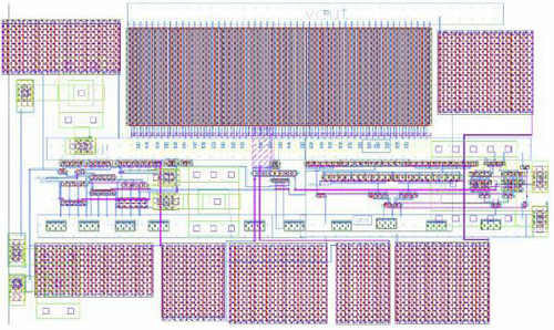
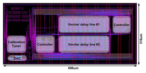
A 1.2ps resolution, 76dB Dynamic Range Time-to-Digital Converter Based on a Tunable Vernier Delay Line
 Enlarge
Yejoong Kim, Suyoung Bang, Dongsuk Jeon
Background: Time-to-Digital Converters (TDC) convert timing information (generally, a pulse width or timing difference between two pulses) into a digital output code. In conventional TDCs using buffer delay lines, the resolution is usually limited to one buffer delay (typically tens~hundreds picoseconds), but Vernier delay lines greatly improve the resolution since the resolution is determined by the difference of the two buffer delays. However, one of the significant problems is that Vernier delay lines are quite vulnerable to variations, as most analog circuits are.
Project: In order to address this issue, we built an auto-calibration process, tunable delay lines, and DAC (Digital-to-Analog Converter). Using a reference pulse width, the calibration controller tries to find an optimum DAC code to generate the appropriate bias voltages for the tunable delay lines. Through this process, most of the process variations (including all the slow variations such as temperature variations) can be effectively compensated, and the team achieved a similar resolution over all the process corners (TT, FF, SS, SF, FS). The worst-case resolution is 1.2ps, which is one of the best resolutions reported so far from 130nm technology.
 Enlarge
Yejoong Kim said, “One of the nice things in this project was that we tried to apply what we’ve learned from other circuit courses like EECS427 (VLSI Design I) and EECS627 (VLSI Design II) to make a complete system. Especially for the digital parts like the controllers, we manually built a standard cell library, performed a timing characterization using ELC (Encounter Library Characterizer), and synthesized the circuits using Synopsys Design Compiler, and did APR (Automatic Place and Route) using Cadence Encounter. In this way, we implemented the fully functional controllers in a relatively short time (a few days), and we have total 15,347 transistors in our circuit. We believe that this is the new record on the device count in EECS413 projects. Because of the large device count, we used various simulation tools: Spectre, Multi-threaded HSpice, NanoSim, and NC-Verilog, according to the required accuracy and simulation speed. If a Pad library had been provided, we could have built a complete chip ready for a tape-out. It was a great experience for us to follow the entire flow in designing a mixed-signal circuit.”